That's getting a little ahead of where I am. Here's the project:
Use a 12-button keypad (like a telephone) with 14 contacts (1 for power, 1 for each of the 12 buttons, and 1 dummy) to enter a 3-digit security code in order to be able to power on a computer. The circuit is connected to the power-on button in the computer, which therefore won't work unless the code has been entered.
The contacts for the 3 digits used for the code are connected to 3 of the 4 AND gates in a 74HC08:
- Gate1 input1 is connected to digit 1 of the code, a 10K pull-down resistor, and GND. Input2 is connected to the input of Gate1 of the 74HC04 inverter, a 10K pull-down resistor, and GND.
The output is connected to input2 of AND Gate2, and also through a diode back to Gate1 input1.
So, Gate 1 input 2 is always HIGH, since the inverter input is always LOW. When the digit is pressed, input1 goes HIGH and stays there due to the diode for latching (see experiment 19). H/H ANDS to H, so input 2 of Gate 2 is H only when digit1 has been pressed. - Gate2 input1 is connected in the exact same configuration as Gate1: 10K resistor and GND, also a diode and gate2 output. Thus, if digit1 has been pushed, input2 is H and if digit 2 is then pushed input1 is H, making output H and latching there.
Output2 goes to Gate3 input 2 as well as back through the latch. - Gate 3 input 1 is connected to a pull-down resistor and GND and to digit3 (no latch). So only if the first two digits have been entered successfully, input 2 is H, and when digit3 is pressed the output3 is H.
Output3 (Gate3 output) goes to Inverter Gate2 input.
Inverter Gate2 output goes to pin2 (trigger) of a 555 timer. H output of AND Gate3 is inverted to L, triggering the timer.
- 555 pin3 (output) is connected to an LED==>10K resistor==>GND and also to the upper coil of the latching relay
- So, when the 555 is triggered, the positive pulse flashes the LED and activates the relay, completing the power circuit inside the computer and allowing the computer to be powered on.
Two other keys of the keypad (* and #) are also in use:
- The * key powers on the circuit, while it is held down. I connects to an LED/resistor/GND to show that power is on, and to the power pins of the ICs (pin 14 of the logic chips, pint 8 of the 555). It also connects through a 100K resistor to pin 7 (discharge pin) of the 555.
- The # key connects to the lower coil on the relay, as well as to an LED/Resistor/GND. So when the button is pushed, the LED lights, and the relay unlatches, disabling the power on the computer
- So, to start the process, press the * key and hold it while entering the 3 digit code, in sequence. LED1 is on while the key is held. LED 2 flashes when the relay is activated. The * key can then be released, and the computer can be powered on. After the computer is powered down, the # key deactivates the relay and it can not be turrned back on again until the code is reentered.
The 555 serves to send a pulse to activate the relay. In addition to the connections already discussed, pin 8 connects to pin 4 (reset), to keep it H while the * button is held. Pin 7 also connects to pin 6 (threshold), Pin 6 also connects to a 10uf capacitor and GND. Pin 5 (control, connects to a .1uf capactor and GND). Pin 3 (output) connects to an LED/resistor/GND in addition to the upper coil on the latch, so it flashes the LED when the 555 is triggered.
Here's the schematic from figure 4-84 on p. 201 of the book:

Here's what I've done on the breadboard so far (a little messy):

I'll post another when I' closer, but it represents the schematic less the keypad.
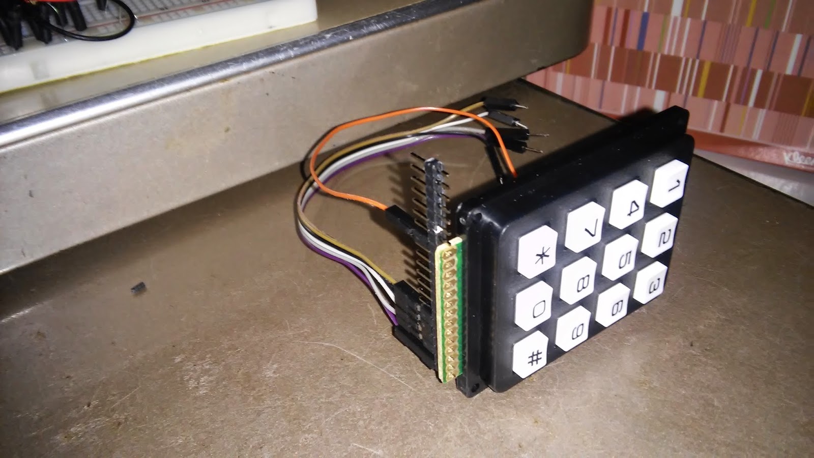
For the keypad, I'm considering soldering a set of header pins, so I can either stick it directly in the breadboard or use F/M jumper wires as depicted below. The top wire is power, The others are randomly connected for now, but they will go to the pads assigned to numbers as discussed above. Other options are to solder wires directly to the pads or to use female headers.
More when I get to soldering.


No comments:
Post a Comment