This experiment is deceptively straightforward. The only issue I had was a bad chip.
First, I mentioned in the last experiment that the slide switch was not breadboard friendly. The pins are not long enough and with only one row of pins it's not stable. I tried taking it apart with the intention of making a breakout board, but that proved to be harder than it should be (I should have left it together). So, I went to Radio Shack and found this. The advantage is that it's a DPDT and has 2 rows of pins, making it more stable.
So with a better switch, I tackled the experiment. Both circuits do the same thing. Debouncing means ignoring errant button pushes. Since latching logic gates set in the first impulse, anything further is ignored. We latch by feeding the outputs of each gate to one of the inputs to the other. The second input is connected to a pull-down (NOR) or pull-up (NAND) resistor and to one side of the switch. The pole of the switch (we only use one) is connected to Vcc (NOR) or GND (NAND).
Each output also powers a low current LED when it's HIGH.
NOR output is LOW unless both inputs are LOW. When the switch is towards a gate's input, that input goes H, making the output L. That gate's LED is off, and one input to the second gate is L. Since the switch is away from the second gate, that input is also L, making the output H, turning on the LED and making one input back to the other gate H, keeping it's output L and it's LED off. Switch to the other gate and one input goes H, making output L and both inputs to the other gate L and it's output H and LED on. It can only be in one state or the other. Debounced.
NAND works similarly. NAND output is H unless both inputs are H. The switch is connected to GND and each gate has 1 input connected to a side of the switch and a pull-up resistor. So, one input is H unless the switch is closed to that side, in which case it's output goes H,turning on the LED and feeding H to one input of the other gate. Since the switch is open to that side, it's pull-up resistor makes the other input H, making the output L, turning off it's LED and feeding L back to the non-switch input of the other gate, keeping it's output H until the switch is moved (or power to the circuit is cut).
Fun and interesting. Here's the video.
Showing posts with label AND. Show all posts
Showing posts with label AND. Show all posts
Saturday, March 21, 2015

Sunday, March 15, 2015
@MAKE Electronics Experiment 20: Keypad Security System Epilogue Part II: Making it Work
Getting past the fact that the 555 won't supply enough voltage, ever, the next question is how can we amplify it. The answer is with a transistor. It took me way longer than it should have to get it to work, because of wiring problems and cooked transistors.
First the wiring: instead of taking 555 Output Pin 3 to the + side of the relay coil, I connected it to the base pin of a 2N2222A transistor (NPN BJT). I then connected + side the relay coil to the 5V rail, and the - side of the coil to the collector pin of the transistor. The emitter pin goes to GND. Initially, I left the LED in the circuit, but since that's connected to GND, the circuit was always completed. I'm sure there's a place I can put it, but it works without it.
After few wrong connections, I still could not get it to work. I was absolutely sure that it was wired correctly. During this process I must have cooked a transistor or two, In desperation, I replaced the transistor again, and it worked.
So, that's the answer: insert a transistor, properly wired, and the voltage that was too low to trip the relay is enough to activate the transistor, allowing 5V to flow from the 5V rail through the relay to the collector, and when the 555 is triggered, the output pin will supply enough voltage to the base pin of the transistor to allow current to flow through to the emitter, completing the circuit.
Here's the video
I'm glad I got this to work. I hate to leave something incomplete..
First the wiring: instead of taking 555 Output Pin 3 to the + side of the relay coil, I connected it to the base pin of a 2N2222A transistor (NPN BJT). I then connected + side the relay coil to the 5V rail, and the - side of the coil to the collector pin of the transistor. The emitter pin goes to GND. Initially, I left the LED in the circuit, but since that's connected to GND, the circuit was always completed. I'm sure there's a place I can put it, but it works without it.
After few wrong connections, I still could not get it to work. I was absolutely sure that it was wired correctly. During this process I must have cooked a transistor or two, In desperation, I replaced the transistor again, and it worked.
So, that's the answer: insert a transistor, properly wired, and the voltage that was too low to trip the relay is enough to activate the transistor, allowing 5V to flow from the 5V rail through the relay to the collector, and when the 555 is triggered, the output pin will supply enough voltage to the base pin of the transistor to allow current to flow through to the emitter, completing the circuit.
Here's the video
I'm glad I got this to work. I hate to leave something incomplete..
Friday, March 13, 2015
@MAKE Electronics Experiment 20: Keypad Security System (Part III--still not working)
This has taken a while. Snow, family visiting, setting up my new generator, an fuel oil spill in my basement, and other events have dominated my attention.
When last we left this, I was convinced that the keypad was sucking current from the circuit. I used this one. The only videos I've seen of people getting this to work use momentary buttons instead of the keypad, I tried to substitute buttons--that didn't help. Testing various locations with my meter, I see that's not the problem
I checked the voltage coming into the first part of the circuit, and then then through the operation. I put a meter set to continuity connected to the relay. If the upper coil on the relay gets 5V, there should be continuity, and 5V to the lower coil should reset it. As you can see in the video, holding the '*' key and entering the code causes the indicator light to turn on for ~1s as designed, but the relay does not flop. The voltage meter shows <4V coming out of the 555--not enough for the relay. If I hit the relay with a jumper wire connected to the 5V rail, the relay flops and there is continuity until I press the '#' key or hit the lower coil with 5V,
Testing various locations with my meter, I see that's not the problem. Here's the video.
The 555 has 4.86V going in on pin 8 and only ~3.7 going out on pin 3. That's the problem, and I don't know what to do about it. I fussed with capacitor and resistor values with no change. For the video, I wound up with ad 1000uf capacitor and a 10K resistor, so pin 3 would have output for longer and I could see it on the meter. I tried various combinations of 2.2, 10, 100, and 1000uf capacitors and 1K, 10K, and 100K resistors--the output stayed under 4V.
Researching, I found this web page, which says that the output on pin 3 will be ~1.7V less than the input on pin 8. Charles' Encyclopedia of Electronic Components Volume 2 says the same thing. I'm going to move on.
When last we left this, I was convinced that the keypad was sucking current from the circuit. I used this one. The only videos I've seen of people getting this to work use momentary buttons instead of the keypad, I tried to substitute buttons--that didn't help. Testing various locations with my meter, I see that's not the problem
I checked the voltage coming into the first part of the circuit, and then then through the operation. I put a meter set to continuity connected to the relay. If the upper coil on the relay gets 5V, there should be continuity, and 5V to the lower coil should reset it. As you can see in the video, holding the '*' key and entering the code causes the indicator light to turn on for ~1s as designed, but the relay does not flop. The voltage meter shows <4V coming out of the 555--not enough for the relay. If I hit the relay with a jumper wire connected to the 5V rail, the relay flops and there is continuity until I press the '#' key or hit the lower coil with 5V,
Testing various locations with my meter, I see that's not the problem. Here's the video.
The 555 has 4.86V going in on pin 8 and only ~3.7 going out on pin 3. That's the problem, and I don't know what to do about it. I fussed with capacitor and resistor values with no change. For the video, I wound up with ad 1000uf capacitor and a 10K resistor, so pin 3 would have output for longer and I could see it on the meter. I tried various combinations of 2.2, 10, 100, and 1000uf capacitors and 1K, 10K, and 100K resistors--the output stayed under 4V.
Researching, I found this web page, which says that the output on pin 3 will be ~1.7V less than the input on pin 8. Charles' Encyclopedia of Electronic Components Volume 2 says the same thing. I'm going to move on.
Wednesday, February 18, 2015
@MAKE Electronics Experiment 20: Keypad Security System (Part I)
Experiment 20 builds on the logic chip exercise in #19 to build a keypad security system. The full experiment ends with hacking into a computer's power button and cutting a hole in the case to attach the keypad. I have several carcasses around that I can use for that, but I think rather than dedicating the system to a computer I don't use I will do the experiment with the case open. I will go as far as cutting the power lines and fixing them to the relay.
That's getting a little ahead of where I am. Here's the project:
Use a 12-button keypad (like a telephone) with 14 contacts (1 for power, 1 for each of the 12 buttons, and 1 dummy) to enter a 3-digit security code in order to be able to power on a computer. The circuit is connected to the power-on button in the computer, which therefore won't work unless the code has been entered.
The contacts for the 3 digits used for the code are connected to 3 of the 4 AND gates in a 74HC08:


That's getting a little ahead of where I am. Here's the project:
Use a 12-button keypad (like a telephone) with 14 contacts (1 for power, 1 for each of the 12 buttons, and 1 dummy) to enter a 3-digit security code in order to be able to power on a computer. The circuit is connected to the power-on button in the computer, which therefore won't work unless the code has been entered.
The contacts for the 3 digits used for the code are connected to 3 of the 4 AND gates in a 74HC08:
- Gate1 input1 is connected to digit 1 of the code, a 10K pull-down resistor, and GND. Input2 is connected to the input of Gate1 of the 74HC04 inverter, a 10K pull-down resistor, and GND.
The output is connected to input2 of AND Gate2, and also through a diode back to Gate1 input1.
So, Gate 1 input 2 is always HIGH, since the inverter input is always LOW. When the digit is pressed, input1 goes HIGH and stays there due to the diode for latching (see experiment 19). H/H ANDS to H, so input 2 of Gate 2 is H only when digit1 has been pressed. - Gate2 input1 is connected in the exact same configuration as Gate1: 10K resistor and GND, also a diode and gate2 output. Thus, if digit1 has been pushed, input2 is H and if digit 2 is then pushed input1 is H, making output H and latching there.
Output2 goes to Gate3 input 2 as well as back through the latch. - Gate 3 input 1 is connected to a pull-down resistor and GND and to digit3 (no latch). So only if the first two digits have been entered successfully, input 2 is H, and when digit3 is pressed the output3 is H.
Output3 (Gate3 output) goes to Inverter Gate2 input.
Inverter Gate2 output goes to pin2 (trigger) of a 555 timer. H output of AND Gate3 is inverted to L, triggering the timer.
- 555 pin3 (output) is connected to an LED==>10K resistor==>GND and also to the upper coil of the latching relay
- So, when the 555 is triggered, the positive pulse flashes the LED and activates the relay, completing the power circuit inside the computer and allowing the computer to be powered on.
Two other keys of the keypad (* and #) are also in use:
- The * key powers on the circuit, while it is held down. I connects to an LED/resistor/GND to show that power is on, and to the power pins of the ICs (pin 14 of the logic chips, pint 8 of the 555). It also connects through a 100K resistor to pin 7 (discharge pin) of the 555.
- The # key connects to the lower coil on the relay, as well as to an LED/Resistor/GND. So when the button is pushed, the LED lights, and the relay unlatches, disabling the power on the computer
- So, to start the process, press the * key and hold it while entering the 3 digit code, in sequence. LED1 is on while the key is held. LED 2 flashes when the relay is activated. The * key can then be released, and the computer can be powered on. After the computer is powered down, the # key deactivates the relay and it can not be turrned back on again until the code is reentered.
The 555 serves to send a pulse to activate the relay. In addition to the connections already discussed, pin 8 connects to pin 4 (reset), to keep it H while the * button is held. Pin 7 also connects to pin 6 (threshold), Pin 6 also connects to a 10uf capacitor and GND. Pin 5 (control, connects to a .1uf capactor and GND). Pin 3 (output) connects to an LED/resistor/GND in addition to the upper coil on the latch, so it flashes the LED when the 555 is triggered.
Here's the schematic from figure 4-84 on p. 201 of the book:
Here's what I've done on the breadboard so far (a little messy):
I'll post another when I' closer, but it represents the schematic less the keypad.
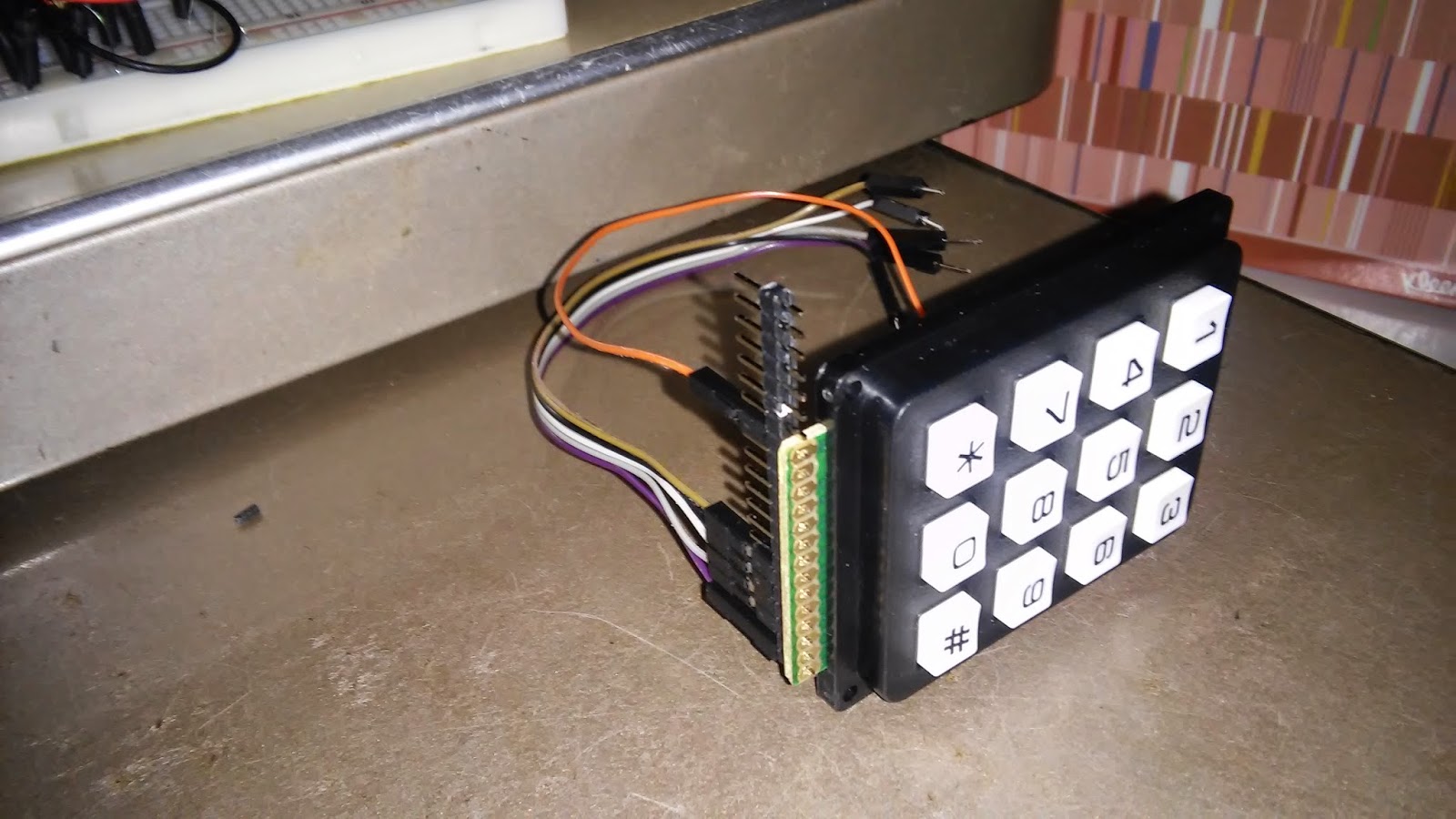
For the keypad, I'm considering soldering a set of header pins, so I can either stick it directly in the breadboard or use F/M jumper wires as depicted below. The top wire is power, The others are randomly connected for now, but they will go to the pads assigned to numbers as discussed above. Other options are to solder wires directly to the pads or to use female headers.
More when I get to soldering.
Friday, February 6, 2015
@MAKE Electronics Experiment 19 - logic chips (Part V)-Finally got my AND chips--more latching
My first post on this experiment said that there isn't much too it. I was wrong. Because, to paraphrase Donald Rumsfield, I had to experiment with the ICs I had not the ICs I wanted, I wound up learning a whole lot. Of course, that is Charles' intent and this book is great. My 74HC08 AND chips arrived, so in this post I will recap what the chapter showed and add a little more about latching,
There is a lot more detail in the chapter on various logic chips and their associated truth tables, and that's very useful.
First step was to do some schematics. I did one for the last exercise in the chapter--latching with an single AND:
The right side is the power supply, as described in Part I (Vcc is regulated 5V). The left side is a self-latching AND gate:
I never would have thought to try any of this if my eBay supplier had delivered the AND chips sooner. I am a lucky man.
See the video.
There is a lot more detail in the chapter on various logic chips and their associated truth tables, and that's very useful.
First step was to do some schematics. I did one for the last exercise in the chapter--latching with an single AND:
 |
| My Eagle Cad Rendition of Charles Figure 4-79, p. 196 |
The right side is the power supply, as described in Part I (Vcc is regulated 5V). The left side is a self-latching AND gate:
- Input 1 is connected to Vcc, so it is always H
- Input 2 is connected to S1. When we press S1, Pin 2 is H. H/H ANDs to H, so the LED lights.
- Without the other connections, the LED would only stay lit as long as the button is pushed. When we let go the pin goes back to L, L/H ANDs to L, and the LED turns off.
- By connecting the output on pin 3 back to the input on pin 2, we keep pin 2 H. The diode blocks any current from S1 from going to the output.
Once we push the button the light stays on, forever--or at least until we disconnect the power. We might want to include another button to turn it off. We could do that by putting a toggle, or perhaps a normally closed pusbutton between Vcc and pin 1. That way, when the toggle is off or the button is pushed, pin 1 would go L, making the output L, and the latch would keep it there (or that's my theory). The toggle is not a great option, because when it's open essentially pin 1 would be floating. Charles says that's not a good idea. I've seen examples where pins are left floating, but I trust Charles. It's kind of like coding an IF construct in any programming language: if you don't deal with all options you may get intermittent strange results. I cover a couple of options to accomplish this in the accompanying video.
Given what I just learned about latching, how about if we add a NAND gate and make one of it's inputs the output on pin3? If we connect the other NAND input to S2, than that input would be L unless the button id pushed. Since only H/H NANDs to L, the NAND output would be H until both the LED is lit (AND output on pin 3 H) and the S2 is pushed. So, we could make the output of the NAND gate input 1 to the AND gate.
- The AND part of the circuit works as before. The only difference is that pin 1 is connected to NAND output instead of to Vcc. Pin 1 is H unless we make it L.
- NAND output is H on power up (S2 open), so AND pin 1 is H.
- We push S1, pin 2 goes H, the output is H, the LED lights and stays lit.
- When we push S2, NAND input 2 is H, making NAND output L (H/H-->L), making AND pin 1 L, making AND output L, turning LED1 off and keeping it that way, but LED2 stays off only momentarily.
Here's the schematic (I omitted the 7805, etc., to reduce clutter):

I never would have thought to try any of this if my eBay supplier had delivered the AND chips sooner. I am a lucky man.
See the video.
Subscribe to:
Posts (Atom)


